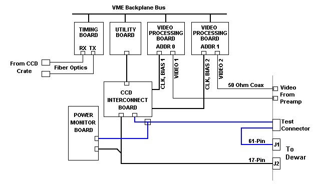
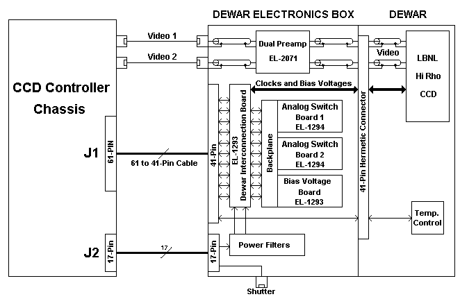
The EL-1274 High Resistivity CCD controller box has been built by the UCO/Lick Observatory Electronics Lab. The controller is built around the San Diego State University (SDSU) rev. 1 board set. There are several aspects that make this controller different from any of the earlier CCD controllers. Most notably, this controller provides a different set of power supply voltages for the bias levels . While all controllers have +5V, +15V, and -15V supplies, due to the characteristics of the High Resistivity CCD (Hi-Rho), this controller has replaced the +35V supply with a +120VDC supply. Also, this controller has an additional -35V supply. This impacts the wiring and the layout of the chassis. Because the Hi-Rho system has been put together using parts from the old Lick Dewar #8 and an unused controller that was originally built for the ESI instrument in Hawaii, this system is unique and very little of it is interchangeable with other controllers.
The SDSU board set.
TIMING BOARD
The SDSU board set is made up of three different boards. First, the TIMING
board, perform all of the timing, control, and communications functions.
The communications and transfer of data occurs over a set of duplex fiber
cables. The fibers connect the controller to a VME bases box that then talks
over a private ethernet link to the data taking computer. The TIMING board
is also used to setup the clock waveforms for the CCD chip. The waveforms
are determined by the CCD Lab and the Lick Scientific Programming Group
(SPG) and then are programmed into the TIMING board.
VIDEO BOARD
The VIDEO board performs three functions. First, it is where the actual
CCD waveforms are generated. Each waveform is built up using two separate
DACs. One DAC is programmed for the high level of the waveform while the
other DAC is programmed for the low level of the waveform. For example,
say the first DAC is programmed to output a level of +9 volts and the second
one is programmed -3.5 volts. By alternately enabling the two DACs the resulting
waveform would alternate between +9 and -3.5 volts with the duty cycle being
determined by the timing of the TIMING board. In this way the waveforms
can be generated to shift the charge both along the columns and the rows.
Each VIDEO board can generate up to twelve separate clocks.
Next, the VIDEO board can generate as many as seven bias levels. As noted
on drawing EL-1277,
the first four outputs are geared toward specific uses such as Vdd and Vr.
The last three are general purpose and can be set anywhere within the specified
range. The bias levels are set and applied to the CCD as required.
The last function of the VIDEO board is to receive the video signal from
the preamp and digitize it via a ADC. This digitized value is then sent
to the VME Crate via the TIMING board during the readout cycle of an exposure.
UTILITY BOARD
The UTILITY board provides general I/O and miscellaneous functions. EL-1276
presents a table of the functions used specifically for the Hi-Rho controller.
Among these functions are a control line for the shutter, a current source
and input for reading the temperature diode mounted in the dewar, and an
analog output to control the heater resistor in the dewar. Also shown are
an analog output at pin A25 to control the front panel temperature meter
and the input and outputs associated with the Lick Power Monitor card.
UCO/Lick Boards
The controller also houses two boards built by Lick. These are the EL-1281 CCD INTERCONNECT board and the EL-1198 POWER MONITOR board.
CCD INTERCONNECT BOARD
This board connects the SDSU VIDEO and UTILITY boards to the output connectors
and the rest of the controller. Viewing both the board schematic and the
EL-1280 Jumper
drawings shows how the INTERCONNECT board is general purpose enough to allow
for just about any configuration of a CCD controller. Each of the jumpers
can be positioned to route it's associated general purpose connection to
the rear connector of the board -or- to instead tie the output pin
to ground. This allows us to add more grounds to the ribbon cable that leaves
the board's output connector when not otherwise used for a signal. In non-standard
applications, we can use wire-wrap instead of jumpers to allow signals follow
any necessary path. On the jumper drawing rectangles around sets of pins
represent shorting blocks while lines represent wire-wrap wires.
POWER MONITOR BOARD
The POWER MONITOR board acts as a power supervisor for the controller. (See
the detailed write-up in the Boards portion of this manual.) It controls
the application and removal of the +/-15 volts from the backplane, controls
the High Voltage application and removal from the Dewar Electronics box,
and turns the analog switches in the Dewar Electronics box on and off. The
general idea is that the HV and analog switches can not turn on until the
+/- 15V is on and the +/-15V can not turn off until the HV and analog switches
are off. This sequence is important to keep wrong voltages off of the CCD
chip. It also monitors the AC input for an under-voltage condition and the
same for the +5V supply. Also, in the case of the +5V supply going too low
a reset signal is sent to the processor on the SDSU Timing board. Again,
these conditions will cause the removal of power to the CCD in the proper
order.
Controller Wring
The front panel of the controller should look similar to both the old style Lick CCD controller and a newer SDSU boxes. On the leftmost panel, is the AC power switch and two toggle switches. The toggle switch on the left is marked 15V and provides a manual means of turning off both the +15V and the -15V supplies. The other switch provides control of the +48 volt supply. These switches are actually inputs to the EL-1183 Power Monitor board. This board contains circuitry to monitor the AC voltage, The +5V logic power supply, the +/-15V supplies, and the +48V supply. Each of these voltages are feed to voltage monitor circuits and if any one of then fall below a set point, the voltages will be removed from the backplane and dewar electronic box in a controlled fashion. The sequence is as follows: first, the +48V supply is turned off and then the +/-15V supplies are turned off. Also, as mentioned, the front panel switches are inputs to this board and can only turn on the supplies if the software inputs to the Power Monitor board are asserted. Again, the application of power is controlled such that the +/-15V supplies must be turned on before the +48V will be allowed to come on. See the description on the EL-1183 Power Monitor for a more complete details.

Blah, blah, blah
